With the development of high power electronic products in the direction of miniaturization, high speed, the traditional FR - 4, aluminum substrates such as substrate material is no longer suitable for PCB industry toward the development of high power, wisdom, application, with the progress of science and technology, the traditional LTCC, DBC technology is gradually replaced by DPC, LAM technology. Represented by LAM, technology of laser technology more in line with the printed circuit board high-density interconnect, fine development. Laser drilling is the front end of the PCB industry and mainstream drilling technology, the technology and efficient, rapid, accurate, and has great application value.
Meriton ceramic circuit board
Horizontal atmospheric pressure CO2 laser excited by the Canadian company to develop and become, compared with the ordinary laser, the output power can be as high as one hundred to one thousand times or so, and made easy. In the electromagnetic spectrum, radio frequency (rf) in 105-109 hz frequency range, frequency of CO2 is accompanied by the military, space technology and development, the development of small and medium-sized power rf CO2 laser has excellent performance, modulation work spontaneously and stability, high reliability, long life and other characteristics. Uv YAG components are widely used in microelectronics industry of the solid material such as plastic and metal. Although CO2 laser drilling process is complicated, the production of microporous aperture than uv YAG solid, but in CO2 laser drilling has the advantages of the high efficiency, high speed, laser micro holes in the PCB market in the process of weight can account for eighty percent.
Domestic laser microporous technology is still in its stage of development, can be put into production of the enterprise is not much. Using short pulses and peak power of laser drilling on the PCB substrate, gathered in order to achieve high density of energy, material instantly remove, forming microporous process requirement, etc. The ablation is divided into both chemical ablation thermal ablation and light. Thermal ablation instantly absorbs high-energy laser refers to the substrate material, to complete the pore forming process. Photochemical ablation is referring to the ultraviolet area more than 2 ev electron volts of high energy and more than the results of the laser wavelength of 400 nm work together. This technology can effectively the destruction of the organic material of long molecular chains, formation of smaller particles, particles under the device suction force, can make the base material forming microporous quickly.
Meriton ceramic circuit board
Today, the country's laser drilling technology has the certain experience accumulation and technical progress. Compared to the traditional drilling technology, laser drilling technology has high precision, high speed, high efficiency and can be large-scale mass punch, suitable for most of the hard and soft materials, tools for lossless, produce less waste materials, environmental protection, no pollution and other advantages.
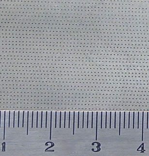
Through laser punching process more binding force with ceramic and metal ceramic board is high, there is no fall off, the phenomenon such as blister, to achieve the effect of growth together, high surface roughness, rough rate at 0.1 mu m ~ 0.3 microns, laser perforation aperture in the 0.15 mm to 0.15 mm, moreover can reach 0.06 mm.